Semiconductor manufacturing demands ultra-clean conditions to prevent defects, contamination, and electrostatic discharge (ESD) damage. Strict cleanroom protocols are essential to maintain yield and product reliability. Here’s a breakdown of key procedures and best practices for semiconductor labs.
1. Personnel Protocols
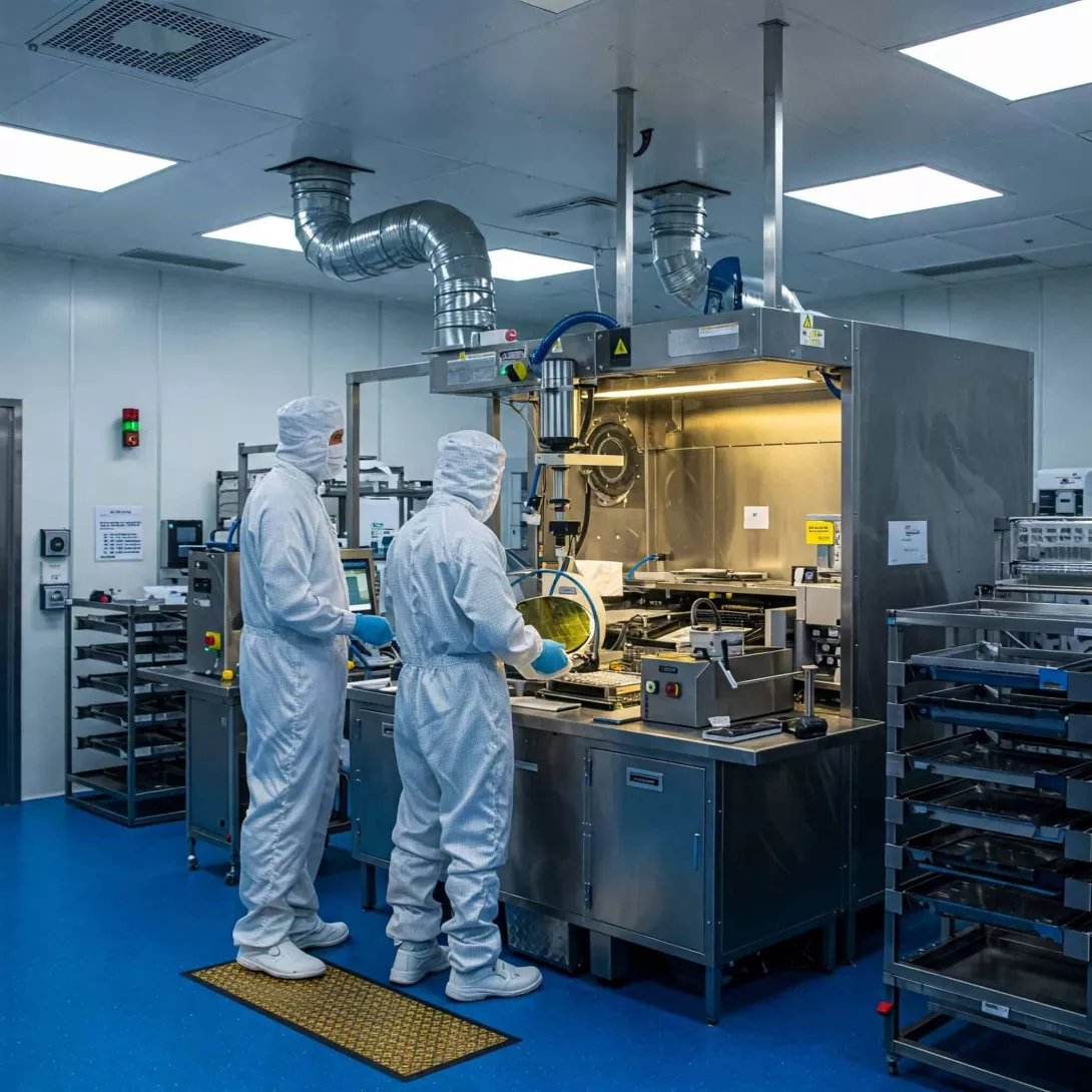
Human activity is the biggest contamination risk in cleanrooms. Proper gowning and behavior are critical.
Gowning Procedures
- Full-body coverage: Wear ESD-safe coveralls, hoods, booties, and gloves.
- Proper donning sequence:
- Step on sticky mat to remove shoe contaminants.
- Put on hairnets and beard covers (if applicable).
- Wear cleanroom suits (zipped fully).
- Put on gloves last (check for tears).
- No makeup/perfume: These can introduce particles and chemical vapors.
Behavioral Rules
- Minimize movement: Fast walking increases particle shedding.
- No touching exposed skin or surfaces: Gloves must remain clean.
- Avoid unnecessary talking: Saliva droplets can contaminate wafers.
2. Cleanroom Entry & Exit Procedures
Entry Steps
- Air shower: Removes loose particles before entering.
- Sticky mat use: Captures foot-borne contaminants.
- ESD grounding: Touch an ESD-safe surface before handling wafers.
Exit Steps
- Dispose of gloves & other single-use items properly.
- Remove garments in reverse order (gloves first, suit last).
- Avoid reusing disposable items.
3. Material & Equipment Handling
Tool & Component Transport
- Use ESD-safe packaging (static-shielding bags, conductive totes).
- Wipe down tools with IPA (isopropyl alcohol) wipes before entry.
Wafer Handling Best Practices
- Always handle wafers with vacuum wands or ESD-safe tweezers.
- Never place wafers directly on surfaces—use cleanroom-certified trays.
4. Cleaning & Maintenance
Daily Cleaning Routine
- Wipe surfaces with low-lint polyester wipes & IPA.
- Replace sticky mats regularly (when >60% covered).
- Use HEPA-filtered vacuums (never brooms or compressed air).
Equipment Maintenance
- Follow SEMI S2/S8 standards for semiconductor tool safety.
- Schedule preventive maintenance to avoid particle buildup.
5. Monitoring & Compliance
Air Quality Checks
- Particle counters: Ensure ISO Class 5 or better (≤3,520 particles/m³ for ≥0.5µm).
- Pressure differentials: Maintain positive airflow to prevent contamination ingress.
ESD Control Verification
- Regularly test ESD flooring & garments (surface resistance <10¹¹ ohms).
- Use wrist strap testers for personnel compliance.
Common Mistakes to Avoid
- Skipping gowning steps (e.g., not wearing hoods).
- Using non-cleanroom-approved materials (e.g., paper, standard plastic).
- Ignoring ESD protocols (leading to damaged ICs).
- Reusing disposable items (increases contamination risk).
Conclusion
Strict cleanroom protocols are non-negotiable in semiconductor labs. By following proper gowning, handling, cleaning, and monitoring procedures, manufacturers can minimize defects, improve yield, and ensure high-quality chip production.
Tags